STRUCTURAL REDESIGN
Tata Electronics Redesigns Dholera Fab Foundation After Soil Complications
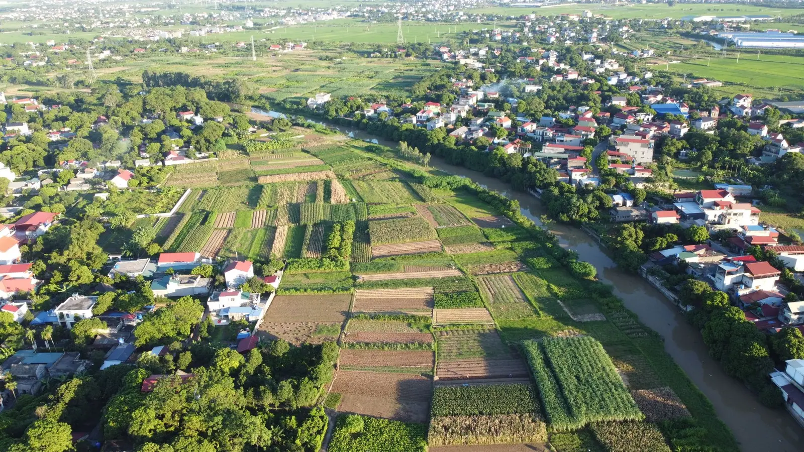
Tata Electronics has initiated a comprehensive redesign of the foundation for its upcoming Rs 91,000 crore semiconductor fabrication plant in Dholera, Gujarat, after updated geological studies found the site's soil conditions to be significantly more complex than earlier estimated. The Dholera site sits on reclaimed land with clay-heavy, saline and silty soil that has a low load-bearing capacity.
| Investment | ₹91,000 crore (~USD 11 billion) |
|---|---|
| Joint Developer | Tata Electronics & Taiwan's Powerchip Semiconductor Manufacturing Corporation (PSMC) |
| Site Soil Issue | Reclaimed land with clay-heavy, saline, silty composition; low load-bearing capacity |
| Experts Engaged | Fugro (geo-data specialist); Cengers (geotechnical consultancy); Geo Dynamics Engineers |
| Redesign Scope | Foundation only; ancillary work repurposed for utility blocks and warehouses |
| Planned Capacity | 50,000 wafers per month at full capacity |
| Targeted Production Start | December 2026 |
| Expected Jobs | Over 20,000 direct and indirect skilled positions |
| Manufacturing Nodes | 28nm, 40nm, 55nm, 90nm, 110nm technology nodes |
| Project Status (as of July 2026) | 50% construction complete; redesigned foundation under construction at full pace |
What Prompted the Redesign
The Dholera site sits on reclaimed land with clay-heavy, saline and silty soil that has a low load-bearing capacity. Semiconductor fabs require highly stable, vibration-free foundations to support precision manufacturing equipment, making any structural miscalculation a long-term risk to operations. The ground is described as clay-heavy, silty, saline, and with low load-bearing capacity, which makes the soil weaker and prone to shifting over time.
Who Made the Decision & Technical Response
To address the challenge, Tata Electronics has brought in global geo-data specialist Fugro and geotechnical engineering consultancy Cengers to reassess the terrain and develop a revised foundation blueprint. The teams conducted detailed soil investigations and recommended an upgraded engineering design tailored to the sensitivities of chip production.
A Tata Electronics spokesperson said: 'Given the unique geotechnical conditions of the region, we have prioritised rigorous planning and engaged world class experts to implement comprehensive design and engineering solutions.'
Construction Impact & Repurposing
Construction of the fab's core building has now resumed at full pace, while earlier groundwork will be repurposed for ancillary facilities such as utility blocks and warehouses. Work already completed will not be scrapped. It will be used for supporting buildings such as power units, utility blocks, water treatment areas, storage, and warehouse spaces. Only the main fab structure will follow the revised foundation plan.
Project Timeline Remains On Track
The redesign is not expected to delay the overall project timeline. Despite the redesign, the company has reiterated that the project remains on schedule and execution is back on track. The target remains to begin chip production by December 2026.
Trial production will begin in December 2026, and commercial production will scale through 2027 and 2028.
Project Scope & Output
The fab, being developed in partnership with Taiwan's Powerchip Semiconductor Manufacturing Corporation (PSMC), is slated to begin chip production by December 2026 and is among India's most ambitious high tech manufacturing projects. This Fab will have manufacturing capacity of up to 50,000 wafers per month and will manufacture chips for applications such as power management IC, display drivers, microcontrollers (MCU) and high-performance computing logic, addressing the growing demand in markets such as automotive, computing and data storage, wireless communication and artificial intelligence.
Broader Dholera Semiconductor Ecosystem
INOX Air Products has commenced construction of a ₹500 crore electronic specialty gas hub in Dholera, Gujarat. The facility will produce ultra-high purity (UHP) gases such as nitrogen, oxygen, argon, and hydrogen — essential for advanced semiconductor fabrication processes and electronics manufacturing. Once operational, the facility is expected to generate over 20,000 skilled jobs, significantly boosting the local economy and the larger semiconductor-manufacturing ecosystem in Dholera and Gujarat.
Development phases
Frequently asked questions
Why did Tata Electronics redesign the fab foundation?
Updated geological studies found the site's soil conditions to be significantly more complex than earlier estimated. The Dholera site sits on reclaimed land with clay-heavy, saline and silty soil that has a low load-bearing capacity.
Which expert firms were hired to assess and redesign the foundation?
Tata Electronics brought in global geo-data specialist Fugro and geotechnical engineering consultancy Cengers to reassess the terrain and develop a revised foundation blueprint. Tata Electronics also brought in Geo Dynamics Engineers.
Will the redesign delay chip production start?
The redesign is not expected to delay the overall project timeline. Despite the redesign, the company has reiterated that the project remains on schedule and execution is back on track. The target remains to begin chip production by December 2026.
What happens to the construction work already completed?
Earlier groundwork will be repurposed for ancillary facilities such as utility blocks and warehouses.
What is the total investment and production capacity of the fab?
The project involves a total investment of ₹91,000 crore. The fab will have manufacturing capacity of up to 50,000 wafers per month.
When will the fab become fully operational?
Trial production will begin in December 2026, and commercial production will scale through 2027 and 2028.
Sources
- Tata Electronics Revises Fab Design For Dholera Soil
- Tata Electronics Redesigns Chip-Fab in Dholera Due to Soil Challenges
- Tata Electronics to Redesign Dholera Fab to Account for Unique Soil Conditions
- Tata Electronics hires top experts to put Dholera fab on a firmer footing
- Inox Air Builds ₹500 Cr Specialty Gas Hub in Dholera & Tata Electronics Fab Redesign
- Tata Group to Build the Nation's First Fab in Dholera
- Tata Semiconductor Plant in Dholera: Chip Manufacturing